Abstract— The budding prominence of automation in technology spread over the multi-disciplinary domains of IoT, Machine Learning, and Artificial Intelligence, necessitate the increased utilization of embedded memories in SoC (System-on-Chip). This directly influences the VLSI industry which is currently witnessing major challenges in the field of Memory Testing.
The ever-increasing competitive SoC market emphasizes the need to cater to faster and efficient testing techniques for memory. Restricting Memory Testing merely to the detection of faults is not enough. Recognizing the significance of response time, performance oriented-ness of memory has become the bottleneck of AI chips.
Consequently, responsibility for the success of AI chips and the IoT industry for its timely delivery in the market with the optimum cost of the end product and best performance delivery lies on the shoulder of the DFT industry. Implementing memory fault diagnosis and enabling its repair must be inculcated at earlier stages of DFT.
This requires special hardware architecture insertion for the repair of defective memory cells which improves the yield of chips. This paper explores one such innovative technology that is implemented with an available Toolset for Memory testing of a consumer SoC. A comparative analysis of this technique with its counterpart has been made w.r.t MBIST insertion time, the time required to test design with memory on Automatic Test Equipment (ATE), and MBIST hardware requirement.
It also provides a brief outlook on Built-in Self-repair for memory and its effect on test hardware. The outlined approach thus addresses the optimization of area and test time, which are the key parameters for any VLSI design.
Keywords— System on Chip, MBIST, memory test architecture, BIRA, ATE
Table of Contents
1) Introduction
A) AI & IoT Industry: Shaping future SoC Trends
The SoC industry trend is experiencing a paradigm shift that is being driven by the growing IoT and AI market. While IoT is about congregating the data through sensors from external environment stimulus, AI is all about making “sense” out of this data and grasping meaningful information to imbibe “intelligence” of its own.
Evolving towards this data-centric era requires tremendous data storage capacity and enhanced processing of data. Implementing and meeting the demands of this developing market mandates the inclusion of greater embedded memory on SoC.
Moreover, to support the dynamic applications of GPU & TPU (tensor processor units), varied types of memory are used on a single SoC. These include SRAM, DRAM, ROM, Flash memory, etc.
Business giants are also assimilating the AI-driven platforms in medical surgery, driverless cars, and automated fueling stations.
For such applications, on-time data streaming, without any packet drop is essential. This can be guaranteed only through the quick responsiveness of embedded memories. Insightful innovations in these two domains are taking the SoC industry towards embedded memory-oriented chips with a greater number of memory macros on a single chip.
However, with novel innovations, come newer challenges, especially for the DFT industry. While the world happily embraces the power of AI, the successful delivery of SoC in the market becomes the responsibility of the DFT industry.
Target accomplishment of these SoCs is guaranteed only when the fabricated IC is validated defect-free. No process technology is 100% accurate. This means certain manufacturing defects can produce faulty chips which can falter the post-silicon functioning of design.
The chips must undergo GO/NO test before it is shipped to the market. Although this is performed post-manufacture, exclusive design for test hardware is introduced in earlier stages of the VLSI design cycle.
The complex integration of memory and logic into the design makes the SoC more vulnerable to manufacturing these defects. Hence, this journey of AI and IoT chips from sand to silicon & silicon to “connected intelligence” is very significant for which, DFT is a critical milestone.
Moreover, the current trend of SoC demands a greater emphasis be put on not only fault diagnosis but also fault repair for a memory test. This is because nowadays, the wafer yield depends greatly on memory SoC yield as it occupies a greater percentage of the SoC area. Having a lower yield of chips greatly affects the cost of the end product.
To address these challenges, the existing memory testing technique called MBIST must be able to administer fault diagnosis as well as memory repair. This is discussed in detail in the next section of this paper.
B) Advancement in MBIST Technique: Meeting the Memory Test Requireents of Future SoC
The VLSI industry has always welcomed mature techniques and tools for memory testing. The most fundamental issue for memory testing is the accessibility of the memory core. Accessing the increased I/O data width from an external tester is a costly affair in terms of time and money.
Therefore, Built-in Self-test is an ideal approach for memory testing. This is termed as Memory Built-in Self-test or MBIST.
This promotes the addition of hardware to follow the DFT methodology. This is also useful for protecting the memory IP [1]. It typically consists of test circuits that apply, read, and compare test patterns- designed to expose defects in the memory device [1].
Certain algorithms are used for this purpose including the “March” algorithm, the checkerboard algorithm, and the varied pattern background algorithm. Despite the advantages offered by MBIST, certain important issues that this scheme does not solve, such as diagnosis and repair. High density, high operating clock rate, and deep submicron technology are giving us more new failures and faults in memory cores [1].
For this, test designers require a diagnosis-supporting mechanism within the MBSIT scheme to enhance product quality, yield, and reliability [1].
Before moving to a discussion on memory diagnosis and repair, the basic MBIST technique implementation in SoC is discussed.
2) General Flow To TEST Memory
A) Steps for memory testing:
- Extract all the required design information from the netlist, and check the design rules, i.e. check the compatibility of design to insert embedded test.
- Plans the Required embedded architecture insertion. (based on cluster ID of memory, the number of memories per controller, the total number of controllers, wrapper, etc.)
- Generates and also verifies all the embedded test architecture in the design such as JTAP, BIST, BIRA, and wrapper, as well as concatenates the generated hardware into the design.
- Insert all scan hardware in the netlist and accomplish pre-layout rules checking.
- Perform post layout DRC checks using formal verification, simulations, and verification.
3) How TO ACCESS MBIST ARCHITECTURE FROM TOP-LEVEL
IJTAG is nothing but an evolutionary JTAG with additional features to simplify the testing architecture. Specifically, IJTAG wraps each IP by a test data register which will be accessed by a segment insertion bit. It is proposed for testing a large number of instruments as well as parallel execution enabled for them, which helps in configuring instruments selectively as needed which ultimately affects test time reduction.
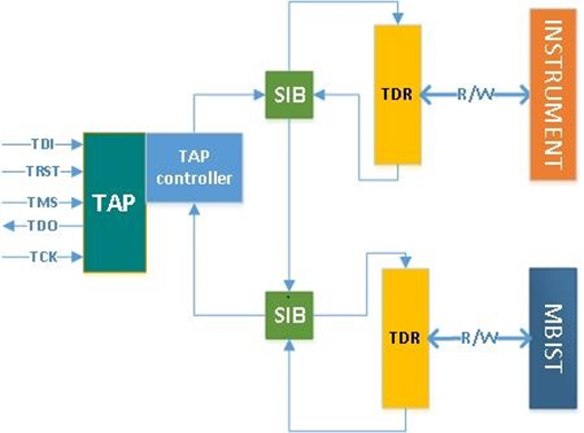
IEEE 1687 consists of the above-mentioned architecture as shown in the figure:
- Instruments: These are the different IPs collaborates in one system.
– eg, PLL, controller, occ, etc
- TAP: Teat access port is Architecture of IEEE 1149.1 which persist five pins to access instruments that are embedded on-chip.
– TDI, TDO, TCK, TMS, TRST
- SIB: A basic key element in IJTAG is the segment insertion bit which is required to activate a portion of the chip’s IJTAG scan path and consequently activate the instrument(s) on that segment of the scan path [4].
- TDR: Test data register act as a read/write interface between TDI to IJTAG instruments
4) Built-in Self Repair- BISR
A) Introduction
As depicted earlier in this paper, the manufacturing yield of SoC can determine the cost of AI or IoT products in the market. Moreover, the memory cores are the most frequently reused IP cores. Ensuring favorable and affordable development cycles of the pre-verified cores in SoC is a crucial methodology. MBIST with diagnosis support is not an essential option. BISR and BIRA are required for this purpose.
- Memory diagnosis has two sets of operations:
- Fault location identification
- Failures analysis, Repair Analysis
Extra redundant or spare cells are added to the main memory. The amount of extra redundant hardware which has to be added is performed during MBIST insertion by the EDA Tool. This is done to have minimum cost and maximum chip yield. Dedicated, powerful algorithms perform such tasks.
The redundancy of different types is possible. This is maybe row-redundancy, column-redundancy, or both. Row redundancy includes adding spare rows while column redundancy includes column redundancy.
Redundancy in 2-dimensional memory testing required the addition of both row and column redundancy. The amount of redundancy to be added depends on the yield required for the SoC.
The latter step helps in improving the design process. The combined BISR is operated in two operational modes [1]:
- BIST Mode
– Main Memory Testing
- BIRA Mode
– Spare memory testing
– Repair of faulty memory cells
Repair analysis pertains to the process of locating the fault site of memory and analyzing the optimum hardware requirement for spare row/column replacement. Repair Delivery corresponds to the process of replacing those faulty memory cells with spare cells.
In the first BIRA mode, MBIST will apply the necessary inputs: Data, RD/WR signal, address, etc. These signals are internally controlled through the BIST controller as mentioned in the previous section. If the fault is detected, the fault signal goes high and the location of the fault is passed to BIRA logic.
B) Repair Delivery
This element of the repair process is responsible for finding those defective sections of memory that must be replaced with available spares. It may be performed off-chip or on-chip. Off-chip repair faces a shortcoming of increased test time. On-chip repair capability provides a powerful technique in which the BIRA engine determines the spare allocation solution. Two approaches for repair delivery can be mainly categorized as:
- Hard Repair: This kind of repair is a permanent instruction repair methodology. This is achieved through fixed programming of fuses. Laser fuse and electrical fuse (e-Fuse) are commonly used fuse types [2].
- Soft Repair: This approach is better as it provides the flexibility to address the repair of defects introduced during manufacture. The instructions are stored in volatile memory which is activated at power-up. This means that the instructions have to be either stored externally or generated during power-up. Storing externally would add to the hardware requirement BIRA provides a mechanism to produce repair instructions at power-up.
The components of BIRA using e-Fuse array, are as follows [2]:
- e-Fuse Array: This is a centralized fuse-pool array that is shared by all memory instances of an SoC. This is possible as not all lower-level hierarchical designs, called “blocks” with memory require memory repair.
- Fuse Controller: The on-chip management of this fuse data allocation across the memory blocks is performed by Fuse Controller. This fuse controller interacts with the BIST engine and BISR engine to perform repair allocation.
- BISR Register: These BIRA registers contain repair information that is stored after the MBIST mode of memory repair flow is executed. The BSR register forms a part of the BISR scan chain. The fuse controller uses this to transfer the repair data from the e-Fuse array pool to memory interfaces [2].
5) Comparative Analysis of Memory Insertion Flow
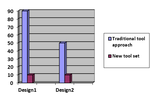
In this section, a comparison between the traditional MBIST insertion flow and current MBIST insertion flow has been made for two designs with a comparable number of memory instances.
The traditional approach followed separate steps for MBIST design rule checks, planning of MBIST insertion hardware, and implementing insertion hardware. The new approach automates the three steps and reduces the required run time.
For illustration purposes, relative data of two different designs have been mentioned in Table I.
Another comparison is made for the same block run with 2 different approaches. In the traditional approach, the embedded test generation and synthesis of the generated design require the maximum amount of time and which is reduced to an extent in the new approach.
The new approach consists of the hierarchical approach on gate-level netlist for 200 or more memory instances because as memories in the SoC increase and its efficient testing plays a crucial role.
Both the techniques are used for testing the memory, but the traditional method persists in WTAP architecture to access the controller from TAP.
WTAP is complex architecture and it acquires more hardware, So, in the new approach, WTAP architecture is replaced by simpler connectivity using the IJTAG concept which basically reduces the drastic amount of time and hardware for testing.
In the traditional approach, the embedded test generation and synthesis of the generated design require the maximum amount of time as it contains WTAP for the connection, which is reduced to an extent in the new approach.
| Analysis 1 | No of Memories | No. of Controllers | Run Time |
| Design 1(With traditional MBIST Insertion Flow) | 110 | 31 | 3 days |
| Design 2 (With new MBIST Insertion approach) | 132 | 18 | 1 hour |
| Analysis 2 | No. of Memories | No. of Controllers | Run Time |
| New MBIST Insertion Flow | 32 | 4 | 1 hours |
| Traditional MBIST Insertion Flow | 32 | 4 | 5 hours |
| Analysis 3 | No. of Memories | No. of Controllers | Time required on ATE |
| New MBIST Insertion Flow | 110 | 31 | 2.78 hours |
| Traditional MBIST Insertion Flow | 132 | 18 | 11 hours |
| No of Memories | No. of Controllers | MBIST Total Area | Total DFT Area | % of MBIST Area | |||
| Design 2 -With new MBIST Insertion approach | |||||||
| 132 | 18 | 7514 | 472050 | 1.59 | |||
| Design 1-With traditional MBIST Insertion Flow | |||||||
| 110 | 31 | 30246 | 1106449 | 2.73 |
| No of Memories | No. of Controllers | MBIST Total Area | Total DFT Area | % of MBIST Area |
| With BIRA | ||||
| 756 | 63 | 130801 | 1999365 | 6.54 |
| Without BIRA | ||||
| 756 | 31 | 100089 | 2019431 | 4.9 |
Conclusion
This paper emphasized the significance of the DFT industry to drive the trending market of AI and IoT towards its successful and timely delivery. BIST with diagnosis support, BIRA, and BISR methodology were discussed briefly. A novel MBIST approach which inculcates BIRA was introduced in this paper.
The new approach was proven to reduce the MBIST hardware insertion time by 98% for design with the roughly same number of memory instances. The ATE time to test the memory design is greatly reduced by 78% for the same design case.
This reduction in time is greatly seen because the hardware requirement has decreased in the new MBIST approach using a Tessent-based toolset.
Finally, a comparison was made that exhibited the hardware increase due to BIRA introduction in design with memory. However, this increase is much more tolerable than the yield loss which would occur otherwise, in the absence of BIRA.
References:
- Laung-Terng Wang. Cheng-Wen Wu. Xiaoqing Wen. and Laung-Terng Wang, “ VLSI Test Principles and Architectures: Design for Testability (Morgan Kaufmann series in systems on silicon)”. Elsevier.
- LogicVision, “Memory Repair Primer- A Guide to Understanding Embedded Memory Repair Options & Issues ”, April 2007
- Mentor, A siemens business ,”Tessent MemoryBIST User’s and Reference Manual. (2009-2018).” 8005 S.W. Boeckman Road, Wilsonville, Oregon 97070-7777
- Asset, Driving Embedded Instrumentation“IEEE P1687 Internal JTAG (IJTAG) Tutorial” Asset, InterTEch
- Applications of IoT in the Medical Industry (Part 2) – Telemedicine – DZone IoT. [online] Available at: https://dzone.com/articles/applications-of-the-internet-of-things-in-the-medi; dzone.com. (2019).
- Meet aggressive time-to-market for AI chips by slashing DFT time « Tessent Solutions. [online] Blogs.mentor.com. Available at: https://blogs.mentor.com/tessent/blog/2019/02/01/meet-aggressive-time-to-market-for-ai-chips-by-slashing-dft-time/ [Solutions, T. (2019). .