Table of Contents
Abstract
Design For Testability(DFT) adds an extra Hardware/Structure in the existing functional design also called MBIST/Scan insertion to get controllability and observability of the design to make it easily testable after manufacturing i.e., post-silicon Soc testing.
Simulation’s pivotal role is to check if the binary response applied as an input that matches the values at the output response of the chip. Based on the matching responses of the circuit, the goodness of the chip will be defined, which in the end concludes the quality of the chip.
In this article, we are going to understand how we can solve the gross simulation failure by understanding and editing the SPF skeleton at the ATPG stage.
Keywords: DFT (Design for testability), ATPG (Automatic test pattern generation), Simulation/Pattern validation, SPF (STIL protocol file).
Introduction
ATPG (Automatic test pattern generation) is the process of generating the test vectors for the particular test mode to check the manufacturing defects, which is further used by simulation tools for validation. ATPG is performed on scan inserted design and the SPF generated through scan insertion. Simulation is the later stage after ATPG, for the validation of the patterns generated in different formats.
All the stages are interdependent on each other.
Refer below figure to check the interdependency of all the stages.
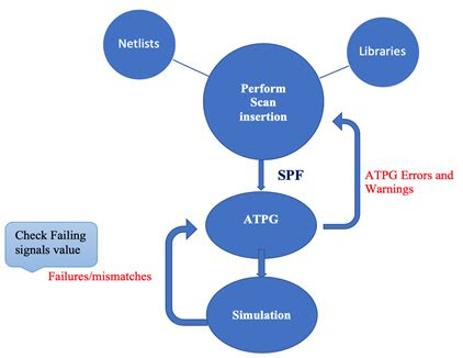
Simulation/Pattern validation plays a vital role in DFT, in order to examine the vectors generated by the ATPG tool.
Once the design is ready with scan inserted netlist, test vectors will be generated and the same vectors will be used for simulation.
If any Error or severe warnings occurs at ATPG/vector generation stage, it can either be solved at the same stage, else we need to jump to the SCAN stage for the required changes which help to clean ATPG issues.
If the pattern simulation failure occurs, we need to analyze the failure and need to do the necessary changes in the ATPG stage like SPF modification to clean up the simulation failures.
What is SPF?
SPF stands for STIL(Standard test interface language) protocol file generated after the scan insertion stage, which consists of all the necessary and basic scan information.
In general words, SPF portrays the information of scan structure, scan chain, initial state value for all the signals for particular test mode and furthermore.
All the above-defined information in SPF is needed to guide the ATPG tool for DRC checks and pattern formatting.
SPF is assigned at the run_drc stage to verify the compatibility of scan inserted netlist with the SPF, it further determines how the scan structure can be used to generate patterns and fault simulations.
Please check below SPF infrastructure segment for a more detailed structure of SPF.
Synopsis Tetramax ATPG flow till DRC
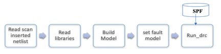
Basic ATPG flow
- Read scan inserted netlist
- Scan outputs are carried forward as ATPG inputs.
- Read libraries
- Read standard cell libraries, target libraries, link libraries, and other necessary libraries in Verilog format
- Build model
- Build the model based on the last unreferenced module read by the read_netlist command, it also flattens the design for further need.
- Set fault model
- Set the fault model transition or stuck based on your requirement
- Run DRC
- Checks the compatibility of scan inserted netlist with SPF for pattern generation.
- If an Error observed, analyze the error and make changes in SPF or netlist accordingly
SPF Skeleton
Let’s begin with the different segments categorized in SPF, described below:
- Signals
- Signal groups
- Scan structure
- Timing
- Procedures
- MacroDefs
The SPF which is described in this article is based on stuck-at faults without compression.
- Signals
It is the first section of SPF containing the definition of all the signals with their type(In, Out, InOut, etc)
2. Signal Grouping
In this section, the signals which were defined in the first part is classified based in a different group based on its type.
The grouping signals further used to provide constraint value at different procedures.
- Below shown are some signal groupings:
“all_in” “all_out”, “all_ports”, “all_bidi”, “_pi”, “_po”, “_si”, “_so”
3. Scan Structure
This section includes the scan chain information like scan chain name, Scan_in, scan_out and scan_enable pin, and also the clock used by that particular chain.
4. Timing
Waveform table is defined in this section which includes the description of the different values provided to different signals like clock period definition, reset value, test mode value, etc.
Waveform table is defined for all the different procedures which are required for different use :
- Default_WFT
- Multiclock_capture_WFT
- Allclock_capture_WFT
- Allclock_launch_WFT
- Allclock_launch_capture_WFT
Note:
- “Default_WFT” is used for loading and unloading of the vectors, or we can say for shifting purpose.
- Among all the above-defined WFT, multiclock_capture is the default capture procedure for all the fault models, always used by the Stuck-at fault model.
- “allclock_*_WFT” is used for at-speed testing, you can the clock frequency based on the requirement for the capture procedure.
5. Procedure
Procedures are defined for the capture cycle of stuck-at and at-speed faults like Multiclock_capture, allclock_capture, allclock_launch, allclock_launch_capture procedures.
Based on which fault model you are using, the capture procedure will be automatically selected.
Example of one capture procedure, and how its structure looks like:
//Default capture procedure in All SPF – multiclock_capture
“multiclock_capture” {
a. W “Multiclock_capture_WFT_”;
// Waveform table for multiclock_capture will be used here
b. C {
i. “all_in” = 00 \r4 N 1011;
//values defined for signal group “all_in”.
//We just need to map the value defined in C statement with the signals mentioned in the “all_in” signalgrouping.
//clk_1 = 0; clk_2 = 0; ScanIn_1 = N; ScanIn_2 = N; Input_1 = N; Input_2 = N;
rstn_L = 1;(Active low reset so it should be 1 to deactivate in capture), scan_enable = 0; (Scan enable should be 0 for capture), scan_mode = 1; test_mode = 1
ii. “all_out” = \r4 X;
//All_output is X, as we do not know its initial value, it will be capture later and automatically observed.
iii. “All_bidi” = \r1 Z;
}
iv. F {
“Scan_enable” = 0;
“Scan_mode” = 1;
“clk_1” = P;
“clk_2” = P;
“rstn_L” = 1;
}
//F section contains the signals which need to be changed after its initial state value or constant value.
//clock defined as 0 in “C section” of procedure to provide its an initial value, we need it to be pulsed.
c. V {
i. “PI” = \11 #;
ii. “PO” = \5 #;
}
}
// Total PI and PO numbers with # is the placeholder for the values which is going to be generated for all the signals.
6. MacroDefs
This division includes the test setup part through which we can initialize the instruction and data bit registers at the TAP/top level.
Also, the test setup is required to provide the values to the signals before the pattern generation starts for the scan mode to bring the chip in its known state like functional mode, test mode, MBIST mode, etc.
What is Simulation failure?
Vectors generated by ATPG applied to the simulation stage to check the validity of the signals and nets for a sanity check of the scan inserted netlist.
If the input vectors provided for simulation don’t match with expected or golden output leads to simulation failure.
It is always necessary to clean the simulation without any mismatch to make sure the perfection of scan insertion.
Simulation Failure debugs and its solution:
To debug the mismatches that occurred during the pattern validation, we need a specific tool to check the waveform signals value like ncsim, Verdi, etc.
To debug, first of all, take the absolute path of the failing register and analyze the value of the mandatory signals like clock, reset, D, SI, SO, Q, etc.
If any X value observed in the signal, then back-trace the particular signal and do this until the source for X generation is observed.
- Clock value X
- Reset value X
- Clock Frequency not correct
Clock value X
- In the below-shown waveform, scan_clk, CLK, Scan_en, reset, test_mode and scan_mode are getting X value after some amount of time extent.
- The initialization value seems to be 0 or 1, and after that, it’s getting X throughout for few signals and some it is having similar behavior for the whole signal.
- First of all, for debugging any simulation mismatches, check all the signal values for mandatory signals which illustrate the scan signals like scan clock, scan enables, scan mode, scan reset, etc.
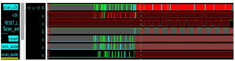
On further back tracing the scan_clk and RESET_L signals, below source test_mode – X and scan_clk – 1 is observed.

It is observed that the value of the clock is ceaselessly 1 and test_mode is X.
Now the question arises in mind that How to resolve? Where to fix it? How to fix it?
So, here are the answer explained below for the above question.
We can force value while performing simulation to temporarily clean it.
Also, to fix the issue without any force given at the simulation stage, we can check the values of the particular signals in SPF used at the ATPG stage.
Here comes the SPF editing part to define the scan_clk and test_mode values.
Earlier the values for scan_clk and test_mode is inaccurately defined in the SPF as shown below:
In this, “All_in” values are defined based on the signals and its position.
As described in the SPF infrastructure section, the values of required scan signals should be set properly in the procedures portion.
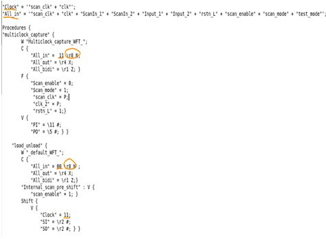
Round marks are drawn on the issue part, and below is the description of that.
Scenario 1:
In “multiclock_capture” procedure, “All_in” values are not correct as shown below:
“All_in” = 11 \r8 N;
//
C {
“All_in” = ‘”scan_clk = 1″ + “clk =1” + “ScanIn_1 = N” + “ScanIn_2 = N” + “Input_1 = N” + “Input_2 = N” + “rstn_L = N” + “scan_enable = N” + “scan_mode = N” + “test_mode = N”‘;
}
F {
“scan_clk” = P; //scan clock is pulsing, it will override the value in C section, so clock will pulse in capture cycle.
}
Solution 1:
C {
“All_in” = 00 \r4 N 1011;
}
F {
“scan_clk” = P;
“test_mode” = 1 //It should be throughout 1 for all the process.
}
Scenario 2:
In “load_unload” procedure – Clock should be pulsing for shift procedures.
In below scenario clock is defined constant 1.
C {
“All_in” = 11 \r8 N;
}
Shift {
V {
“Clock” = 11;
} }
Solution 2:
C {
“All_in” = 00 \r4 N 1011;
}
Shift {
V {
“Clock” = PP; // clock should be pulsing while shifting
} }
Scenario 3:
If the scan clock frequency is different than the required frequency, then change the clock period in _WFT table, as shown below:
“scan_clk” { P { ‘0ns’ D; ’35ns’ U; ’65ns’ D; } }
“clk” { P { ‘0ns’ D; ’25ns’ U; ’75ns’ D; } }
Change the period in ns for the up and down section of the respected scan clock according to the required frequency.
SPF is also used to feed instructions and data bits to the UTDR (user-defined test data register bits) and for initialization/test setup purposes as well.
Conclusion
With the increase in technology nodes, Silicon industry testing has become challenging.
To deal with the failures in SoC we need to invest a significant amount of time and effort.
The above article presents different methods to solve the SoC failures efficiently by performing the modifications in the SPF file.
References
- TestMAX™ ATPGandTestMAXDiagnosisUserGuide, VersionQ-2019.12,December2019
- P1450.1 IEEE Standard Test Interface Language (STIL) for Digital Test Vector Data Design Extension P1450.1 Working-Draft 14, Aug 1, 2002
- Rahul Malhotra∗, Sujay Deb†, Fabio Carlucci‡, “A novel approach to Reusable Time-economized STIL based pattern development” 2015 IEEE
- Micross component “STIL Language Test Vector Format (Simplified)”
- STIL-based Semiconductor Test Action Group (SSTAG), IEEE Std 1450.0-1999, Revision 6.20 Oct. 17, 2011